

")
In today’s competitive and rapidly changing electronic market, the speed and effectiveness of product testing has a significant impact on time-to-market and on final product quality. The increasing complexity of integrated circuits (IC) and multi-layer printed circuit boards (PCB) cause a lot of problems with structural and functional testing of electronics. We can point some of them as follows:
- No access to IC pins and internal PCB layers to measure electric parameters
- Complex structure and long preparation time of tests
- Difficult automation of tests’ generation and results analyzes
- Limited fault coverage and diagnostics
and last but not least
- Integration of micros, flash memories, PLDs, FPGAs in-system programming in testing process
Existing test methods as functional testing and in-circuit testing (ICT) are losing their effectiveness due to impact of new technologies – increasing integration scale and complexity of electronics. So it’s necessary to change approach to testing and quality control. It’s necessary to take into consideration test problems since the beginning of development process - simple to design-for testability (DFT). Boundary-Scan (B-S) is one of the most effective methodologies available today for testing and in-cicuite programming. It base on build-in ICs structure special hardware that simplifying allows to set and read signals on/from internal pins.

Structure of IC with B-S implementation
Boundary-Scan testing was originally devised by an independent committee of professionals from Philips,BT, GEC,TI and others, known as JTAG (Joint Test Action Group) which held a series of meetings throughout the late 1980s. In 1990 it became the IEEE1149.1 standard. Since that time B-S gradually gained in popularity as IC silicon vendors provided more devices compiant with the IEEE1149.1 standard. Today, a great many B-S devices are availble and thousands of production lines around the world use B-S routinely in board testing and in-system programming.
To comply in a standard a device must include:
- 4-wire (5-wire if optional reset signal is included) Test Access Port (TAP)
- Internal B-S cells for each pin
- Associated internal B-S registers
- Additional multiplexing circuity
In addition, the device vendor must provide Boundary-Scan Desription Language (BSDL) files that fully describe the B-S implementation in the associated device. This is a key to automation of test generation and performance. So …
To make testing with B-S method possible, first it’s necessary to use B-S compatible devices in a project. This requirement is easy to meet – most complex ICs has B-S build-in. Moreover, to achieve good test coverage, it’s not necessary to have all devices equipped with B-S. There may be clusters consisting of non-B-S parts that will be testable despite the lack of direct B-S access. It take place for example when PCB including memories is controlled, observed and thoroughly tested from just one or few B-S devices.

B-S on board chain test infrastructure
Next, it’s necessary to design PCB to allow access to B-S devices placed on it. It’s simple to pass this requirement by interconnecting B-S components in a chain or multi-chains on a PCB. This is done by sequentially connecting the B-S Data Output (TDO) pin on one device to the B-S Data Input (TDI) pin on other device, and so on. To control this so called test infrastructure which includes the shifting operations etc., each B-S device is connected to Test Clock (TCK) and Test Mode Select (TMS) signal. The scan chain provides electrical access , from serial TAP interface to every pin on every IC that is a part of chain. In normal operation B-S compatible Ics performs its intended function as though as B-S circuit were not present. However, when testing or in-circuit programming is to be performed, the device scan logic is activated. Then data can be sent to the IC and read from it using the serial interface. This data may be used to stimulate the device core, drive signals outward to the PCB, sense the input pins from the PCB or sense the device outputs. The scan modes of operation provide the ability to test boards or even systems from manufacturing structural faults and to perform in-system device programming – all via the standard JTAG TAP.
Taking into consideration that pin B-S cells are inside a silicon structure, testing with B-S technology is deeper than with “bed-of-nails” fixture – connections between internal cells are checked instead of external pin to pin.
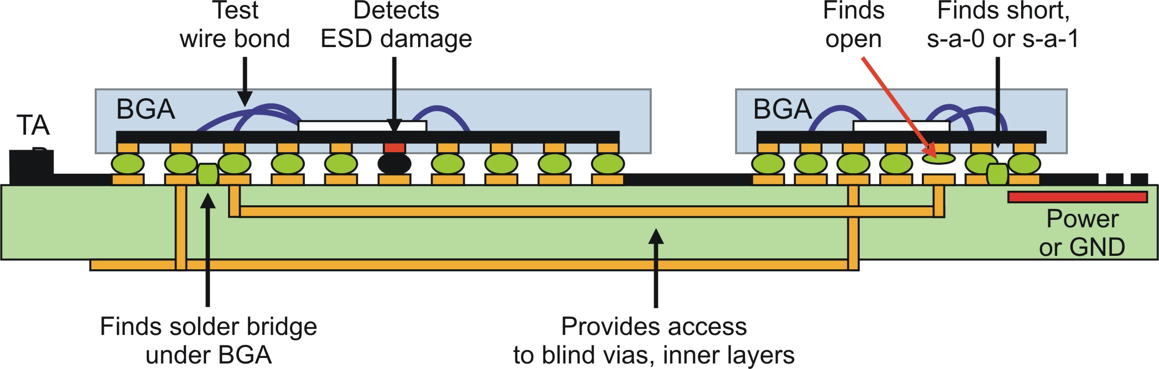
Faults possible to detect in B-S technology
To perform B-S tests and to analyze results PCB has to be connected to host PC via dedicated B-S Controllers with serial TAP interfaces. In addition special digital I/O scan modules extend B-S facilities with on board connectors testing possibilities. Next step can be testing of complete systems consisting of several boards.

Structure of Testing Chain Based on Boundary-Scan Technology
Software available for PCs allows to automatically or semi-automatically generate tests, performed them, visualize and analyze results. JTAG Technologies offers all hardware and software components for B-S testing infrastructure.
B-S testing process can be integrated within automatic test equipment (ATE). JTAG Technologies works with any vendor of in-circuit testers (ICT), flying probes (FPT) or functional testers (FT).
JTAG technology founders were engaged in B-S technology and IEEE1149.1 standard development since the beginning. This standard defines JTAG boundary-scan which was first released in 1990 and has been updated twice since then. The standard defines test logic for inclusion within integrated circuits which can be used at the board-level to conduct precise structural testing and in-system programming.
Since the release of the IEEE 1149.1 specification, four other standards have been developed extending it for specific purposes:
- IEEE 1149.4 – defines analog boundary-scan
- IEEE 1149.6 - expands boundary-scan's testing capability beyond the original digital realm
- IEEE 1532 - sets up a common descriptive format for programmable devices like PLDs and FPGAs
- IEEE 1149.7 - reduces the pin count and enhancing the functionality of the link between 1149.1 test systems and targets.
Additionally there are a number of ongoing efforts to extend JTAG boundary-scan even further. Among these are:
- IEEE P1149.1-2013 - superset and update of 1149.1
- IEEE P1149.8 – an extension to combine B-S technology with capacitive plate sensor technology
- IEEE 1581 - a test extension for memory devices
- IEEE P1687 - an extension to access built-in device-level test instruments
- SJTAG - an extension for system-level testing
JTAG Technologies will work closely with all of these efforts to maintain that state-of-the-art edge.